Viewing entries tagged
nanotechnology

Doping and Designer Materials

Comment

Doping and Designer Materials

Writer: Makeen Shafer

Pictured: Silicon wafer [1]

Ever wondered how a physical computer chip has information on it? Or how a solar panel turns light into electricity? Well the answer, in many cases, is a process called doping.

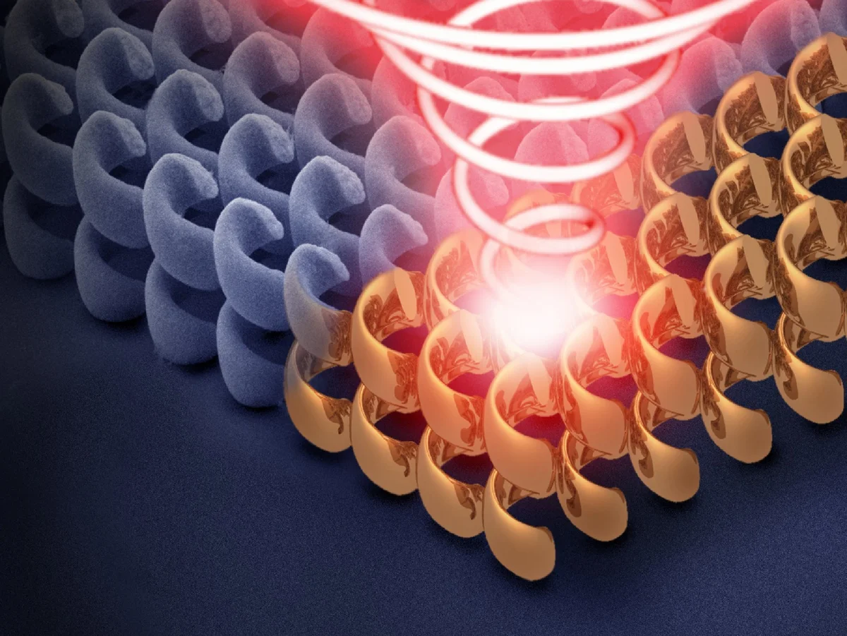
In materials science, doping is the highly tunable process that unlocks the hidden potential of ordinary materials. It's the art of adding precise, tiny, amounts of impurities to a substance to drastically transform its properties. Like salting pasta water, a little bit of doping goes a long way.

The star of modern doping is the semiconductor, its most famous being silicon. By itself, silicon is a poor conductor and a poor insulator of electricity, but with as few as one impurity atom per million silicon atoms, its conductivity can increase by over a thousandfold [2].

To understand how it works, let's take a step back. You might’ve learned in chemistry that different elements behave differently depending on their outermost valence electrons. For a material like silicon with four valence electrons, the impurity introduced, called a dopant, will have either one more valence electron (phosphorus) or one less electron (boron) [3]. This added electron (or “hole” where an electron is missing) in a system of silicon creates a mobile charge carrier, something that can move, in a material where there otherwise were no charges able to move [3]. Think of it like a football stadium where every seat is taken: when an electron is added, a new person can walk freely across the aisles, and when an electron is removed, a seat is freed up that anyone can move to.

Depending on whether the silicon was doped by increasing or decreasing electrons, an n-type semiconductor (more negative charge) or a p-type semiconductor (more positive charge) is created [3]. 

The real magic happens when p-types and n-types are put together. The simplest configurations make up diodes, components where electricity only flows in one direction from n to p, and transistors, the building blocks of computers [4]. For a chip, diodes control current flow and transistors control the 1s and 0s. For a solar cell, when light knocks electrons off an atom, the diode pushes electrons to the n side, building up electricity [5]. 

The GPUs sold by companies like NVIDIA use this same principle: thin silicon wafers are coated with an exact pattern of billions of p-type and n-type regions stacked on top of each other to make a massive system of transistors [6].

But doping goes far beyond semiconductors and chips, it’s everywhere! Just to name a few devices, catalytic converters, fiber optic cables, lasers, and even glow-in-the-dark toys are made using doped materials [7][8][9][10]. Superconductors, for example, are made by specially tuning the total amount of valence electrons (called the fermi level) in a material, a perfect job for doping [11]. Doping doesn’t just involve electronic properties, but can also have to do physical and mechanical properties. For example, tough ceramics (like in dental implants or ceramic knives) can be made by taking zirconia, a brittle material that wants to self-destruct, and adding yttria molecules, providing larger atoms that lock the zirconia in place and prevent it from cracking[12][13].

Using doping, the future of materials science might not depend on discovering new materials, but on tuning the ones we already have. From advancing computers and technology to improving everyday objects, none of it would be possible without clever and atomically precise doping: making humble molecules and elements into designer materials.

References

[1] Scientists grow “perfect” atom-thin materials on industrial silicon wafers. (2023, January 19). Nano Magazine - Latest Nanotechnology News. https://nano-magazine.com/news/2023/1/19/scientists-grow-perfect-atom-thin-materials-on-industrial-silicon-wafers 

[2] Silicon Resistivity. (2018, October 1). UniversityWafer, Inc. https://www.universitywafer.com/silicon-resistivity.html

[3] The Complete Guide to Doping in Semiconductors: What Is it and Why Is it Necessary? (n.d.). Retrieved October 30, 2025, from https://www.waferworld.com/post/the-complete-guide-to-doping-in-semiconductors-what-is-it-and-why-is-it-necessary

[4] P-N Junction: Semiconductor Interface | UniversityWafer, Inc. (2018, October 1). https://www.universitywafer.com/p-n-junction.html

[5] Photodetectors. (n.d.). http://hyperphysics.phy-astr.gsu.edu/hbase/Electronic/ligdet.html

[6] What are P type and N type Silicon Wafers? | WaferPro. (2024, January 10). https://waferpro.com/what-are-p-type-and-n-type-silicon-wafers/

[7] bluefire. (2021, October 8). Noble metal-free catalysts compared to catalysts containing noble metals – A question of recycling—Blue Fire. https://blue-fire.org/en/noble-metal-free-catalysts-compared-to-catalysts-containing-noble-metals-a-question-of-recycling/

[8] Introduction to Fiber Doping Techniques. (n.d.). https://www.gohecho.com/introduction-to-fiber-doping-techniques

[9] Laser Crystals – rods, slabs, disk, neodymium, ytterbium, erbium, thulium, holmium, cerium, titanium, chromium. (n.d.). https://www.rp-photonics.com/laser_crystals.html

[10] Lisensky, G. C., Patel, M. N., & Reich, M. L. (1996). Experiments with Glow-in-the-Dark Toys: Kinetics of Doped ZnS Phosphorescence. Journal of Chemical Education, 73(11), 1048. https://doi.org/10.1021/ed073p1048

[11] Tao, Y.-L., Zeng, W., Fan, D.-H., Liu, Z.-T., & Liu, Q.-J. (2025). Comprehensively understand the mechanism of doping to enhance the superconducting transition temperature of H3S under high pressure. Applied Materials Today, 43, 102653. https://doi.org/10.1016/j.apmt.2025.102653

[12] An Introduction to Yttria Stabilized Zirconia. (n.d.). https://www.preciseceramic.com/blog/an-introduction-to-yttria-stabilized-zirconia.html

[13] Kumar, A., Kumar, P., & Dhaliwal, A. S. (2021). Structural studies of zirconia and yttria doped zirconia for analysing it phase stabilization criteria. IOP Conference Series: Materials Science and Engineering, 1033(1), 012052. https://doi.org/10.1088/1757-899X/1033/1/012052

Comment


GUM GUM: Recent Research Produces Rubbery Material to Replace Human Tissue

Comment

GUM GUM: Recent Research Produces Rubbery Material to Replace Human Tissue

“GUM GUM BAZOOKA!” (Eiichiro, 1999) the protagonist of hit anime One Piece, Monkey D. Luffy, howls to deliver the finishing blow on his enemy.

As watchers of the acclaimed series know, Luffy’s power is that of the gum-gum fruit, which makes his body act as rubber. This seems like something only to happen in an anime, and while it is likely best that rubber bones stay relegated to that fictional, animated world, recent nanostructures and materials research could provide humans with a multipurpose, synthetic, rubbery substance that works in accordance with the human body. At Chalmers University of Technology in Sweden, researchers in the chemistry, chemical engineering, and applied physics departments have discovered a rubbery substance that has the potential to replace human tissue (Rajasekhara et al., 2019). 

In order to create an synthetic elastomer (material of a solid state but with relatively high amounts of elasticity) that could agree with the human body, scientists rethought the process of making elastomers. Previously, researchers made elastomers by randomly linking polymers - materials created by the linking of macromolecules - together. To create elastomers that are compatible with the human body, they sought a more organized approach. This new elastomer would be used as synthetic tissue, so its creators used a technique called ordered structuring to connect polymers with collagen and elastin, two fibrous proteins prominent in human skin (Rajasekhara et al., 2019).

With the help of state-of-the-art nanostructuring technologies, ordered structuring now makes the creation of elastomeric substances possible. This allows the surface to be lined by a material (namely what would be in contact with organs) with antibacterial peptides, making the elastomer resistant to bacteria so that it will not be damaged by the natural bacteria present in humans. One of the current applications for this elastomer involves catheter tubes. The material is able to carry medicine or blood while remaining decontaminated and also not killing the bacteria. This is helpful because there is an increasing trend of bacteria becoming antibiotic resistant , so it is becoming harder to eliminate them (“Nanostructured rubber-like material…”, 2020). This synthetic elastomer tube does not result in bacteria death, rather bacteria removal.

Beyond bacterial resistance, the elastomer has a variety of unique properties. Its soft and elastic nature means that it can be injected into the body by a cannula or 3D printed into a specific shape, and its nanopores can be filled with medicine to allow the synthetic tissue to cater to patients’ specific needs (“Nanostructured rubber-like material…”, 2020).

In theory, these biological elastomeric tissues could be used to create a being with rubbery bones. But, let's leave the gum-gum fruit abilities to Luffy and appreciate the material for its potential to revolutionize medicine.

References:

Eiichiro, O. (Oda), & Konosuke, U. (Uda). One Piece. Toei Animation.

Nanostructured rubber-like material with optimal properties could replace human tissue. (n.d.). ScienceDaily. https://www.sciencedaily.com/releases/2020/03/200316090334.html 
Rajasekharan, A. K., Gyllensten, C., Blomstrand, E., Liebi, M., & Andersson, M. (2019). Tough Ordered Mesoporous Elastomeric Biomaterials Formed at Ambient Conditions. ACS Nano, 14(1), 241–254. https://doi.org/10.1021/acsnano.9b01924

Comment


Attacking Cancer: A Golden Opportunity

Comment

Attacking Cancer: A Golden Opportunity

You don’t have to be a historian to grasp the significant impact gold has made in the world. From a sought-out treasure to a method of currency, there’s no doubt that this element is one of the most influential metals in human history. Yet, a much less known aspect of gold is its incredible potential in biomedicine. This is especially true of gold nanoparticles in the context of cancer.


Cancer is a condition wherein cells proliferate and divide in an uncontrolled manner. [1] While cancer can often be treated, the side effects of those treatments can be severe and can include possibly hurting non-cancer cells and the immune system. Inducing hyperthermia, or causing a part of the body to heat up, has been shown to have an anticancer potential as it can lead to programmed cell death as well as make tumors more susceptible to radiotherapy. Yet, a central issue arises: unless the heat is localized, other parts of the body can be harmed. This is where gold nanoparticles come in. [2]


In the simplest terms, gold nanoparticles are small pieces of gold. Very small pieces of gold. As a result, gold nanoparticles have a lot of different properties compared to, say, a block of gold that we often think about when talking about the element. For instance, gold nanoparticles are not yellow: particles less than 100 nm are red while bigger particles are blue/purple. [3] These nanoparticles have amazing properties which allow them to act as a contrast in CT scans or assist with drug delivery. [4] Yet, one of the most fascinating applications of these gold nanoparticles is their use in photothermal therapy. Because the blood vessels near the tumor site are often leaky, gold nanoparticles that have been placed in a cancer patient's body will passively concentrate near a tumor. Once they have concentrated, they can be activated by near-infrared light, a special type of light which can easily pass through human tissues. The gold nanoparticles will absorb the light energy and convert it to heat energy near the tumor, essentially stimulating the cancer cells’ deaths. [2]


Has this technique been tested in humans? In fact, yes–a clinical trial done at Mt. Sinai hospital which used gold-silica nanoparticles to treat prostate cancer patients revealed no severe side effects from the treatment. After the gold nanoparticles had concentrated at the tumor site of the patients, they were irradiated by near-infrared light from optical fibers. These nanoparticles absorbed the light and heated the tumor site, essentially destroying it. [5]


The promise of such a localized treatment strategy is encouraging. Hopefully, further research can be done to explore this opportunity that is, indeed, worth its weight in gold.


References

[1] Gupta, N.; Malviya, R. Understanding and advancement in gold nanoparticle targeted photothermal therapy of cancer. Biochimica et Biophysica Acta (BBA) - Reviews on Cancer [Online] 2021. 1875, 188532. https://www.sciencedirect.com/science/article/pii/S0304419X21000305?via%3Dihub (accessed November 2021)

[2] Vines, J.B.; Yoon, J.-H.; Ryu, N.-E.; Lim, D.-J.; Park, H. Gold nanoparticles for photothermal cancer therapy. Front. Chem. [Online] 2019. 7, 167. https://www.frontiersin.org/articles/10.3389/fchem.2019.00167/full (accessed November 2021) 

[3] Sztandera, K.; Gorzkiewicz, M.; Klajnert-Maculewicz, B. Gold Nanoparticles in Cancer Treatment. Mol. Pharmaceutics [Online] 2019. 16, 1-23. https://pubs.acs.org/doi/10.1021/acs.molpharmaceut.8b00810 (accessed November 2021)

[4] Wang, S.; Lu, G. Noble and Precious Metals - Properties, Nanoscale Effects and Applications. In Applications of gold nanoparticles in cancer imaging and treatment; Intechopen: Online, 2017.

[5] Stephens, M. PhysicsWorld. https://physicsworld.com/a/gold-nanoshell-based-cancer-treatment-is-safe-for-the-clinic/ (accessed November 2021)

[6] Pxfuel. https://p1.pxfuel.com/preview/830/131/627/cancer-cells-cells-scan-electron-microscope-scan.jpg (accessed November 2021)

Comment