Abstract
The objective of this study was to fabricate 3D micro/nano-structures with an even distribution of single-walled carbon nanotubes (SWCNTs). We utilized two-photon polymerization by means of a pulsed femtosecond laser for fabrication and Raman microscopy for the detection of carbon nanotubes in the structures. In order to test the capability of our laser, we fabricated an assortment of interesting microstructures such as an 8 micron gear, 7 micron dog, and a 100 nm diameter nano-wire. We believe that this study will open the door to the fabrication of even more intricate micro-structures with an even embedment of carbon nanotubes for practical purposes.
Introduction
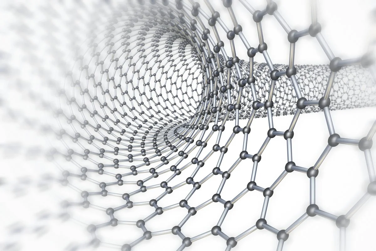
Two-photon polymerization (TPP) is a well-established method used to fabricate intricate 3D micro/nano structures from polymers. These 3D structures have vast potential in applications such as micro-electromechanical devices, sensors, and targeted drug delivery systems. However, it remains necessary to functionalize and enhance the mechanical properties of these polymer micro-structures for practical applications. To this end, single-walled carbon nanotubes (SWCNTs) are critically acclaimed as ideal fillers to enhance mechanical properties of the polymer due to their high Young’s modulus (up to 1.5 TPa), high tensile strengths (up to 63 GPa), high aspect ratios (up to 106), and small diameters (~ 1 nm) 1. In this report, we establish a novel way to evenly embed SWCNTs into 3D micro/nano polymer structures by means of TPP.
Dispersing SWCNTs Evenly in Photoresin
Our photoresin consisted of 0.01 weight % SWCNTs, 96.67 wt % of R712, and 1.67 wt % of photoinitiator and photosensitizer. SWCNTs were evenly distributed in the photoresin by sonicating the mixture for 2-3 hours. After taking the UV spectrum of the photoresin (as seen in Figure 2), we observed a high absorption below 390 nm and low absorption in the IR region, enabling the photoresin photopolymerizable for two-photon polymerization.
Two Photon Polymerization
A Ti:Sapphire pulsed femto-second laser at 780 nm and an intensity of 7 mW was utilized to excite two-photon absorption on the SWCNT dispersed UV photo-polymerizing resin. It took two photons to successfully photo-polymerize the resin, because our photo-resin exhibited a high absorption at 390 nm, and our laser operated at 780 nm. This only occurred at the focus spot of the laser where the photon intensity was highest (see Figure 3). In this manner, point-by-point nanometric volumes of photo-resin were photopolymerized following the trajectory of the focus spot (whose movement was dictated by a pre-programmed CAD file). An assortment of interesting micro/nano-sculptures with an even dispersion of SWCNTs was obtained.
Fabricated Microstructures
Figure 4 shows a few examples of micro-sculptures that I fabricated this summer using two-photon polymerization. All of these structures exhibited a uniform dispersion of SWCNTs.
SWCNTs Embedded in Micro/Nano-Structures
The uniform embedment of SWCNTs in our fabricated micro/nano-structures was detected by Raman Microscopy instrumentation (Raman-11).
To this end, a laser at a wavelength of 785 nm, 10 s exposure time, and intensity of 0.56 mW was utilized. Our sample was placed on a glass substrate and exhibited Raman scattering when eradiated with the laser. The Raman scattering was separated from the Rayleigh scattering through a filter and split into its different frequencies at a grating. The CCD camera then analyzed the Raman signal and constructed a graph of Raman signal vs. wavelength. By using our computer, we were able to input a certain frequency and assign a color to the corresponding Raman intensity at that frequency. We selected the Raman intensity at the G-band frequency to be white (1590 cm-1) and every other Raman intensity signal to be black. The white color then represented a high G-band intensity (hence, a high concentration of SWCNTs). From this information, point-by-point, the computer reconstructed our Raman image by analyzing whether or not the sample had a high Raman intensity signal and assigned a white color to that pixel. If the image resembled our sample, then we had a uniform dispersion of SWCNTs.
As seen in Figure 5, by comparing the SEM image, Brightfield image, and Raman image of the micro bull and nanowire, we observed a uniform dispersion of nanotubes. Furthermore, by taking the Raman spectra on and off the structure, a sharp peak at the G-band occurred on the structure, while no signal occurred off the structure indicating nanotubes only exist on the structure.
Alignment of SWCNTs in Nano-wires
SWCNTs were found to be aligned along the axis of the fabricated nano-wires as observed by polarized Raman microscopy. To this end, we observed that the strongest Raman signal arose when the nano-wire was parallel to laser polarization, and the lowest signal occurred when the nano-wire was perpendicular. Figure 6 shows the G-band Raman intensity vs. degree of nano-wire orientation. While SWCNT alignment may be due to spatial confinement, the reason behind their alignment is still being researched by my research team at Osaka University today.
Conclusion
We have successfully demonstrated 3D micro/nano fabrication of a SWCNT polymer matrix using TPP and elucidated that SWCNTs were embedded in micro structures and aligned along the nanowire axis. We believe that these methods will open the door to a variety of applications needing SWCNT reinforced micro-structures such as drug delivery devices, sensors, and MEMs in the future.
References
- Coleman, J.N. Carbon 44. 2006, 1624–52.
- Ichida, M. Appl. Phys. A. 2004, 78, 1117–20.

